

Increased demand for InP semiconductors due to the development of 5G
Cost reduction is required while maintaining the quality of InP semiconductors.
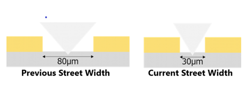
While InP semiconductors have high functionality and high performance, they still have the problem of high cost. Therefore, semiconductor manufacturers have increased the die integration rate per InP wafer to reduce costs. The street width (cutting width) of the wafer is 50 μm or less, and the die size on the wafer is 170 μm × 170 μm. The narrower the street width, the more the wafer can be used without waste, so it‘s required to singulate wafers with a narrow street width with high precision.
Proposing a diamond scriber suitable for InP wafers with narrow street width
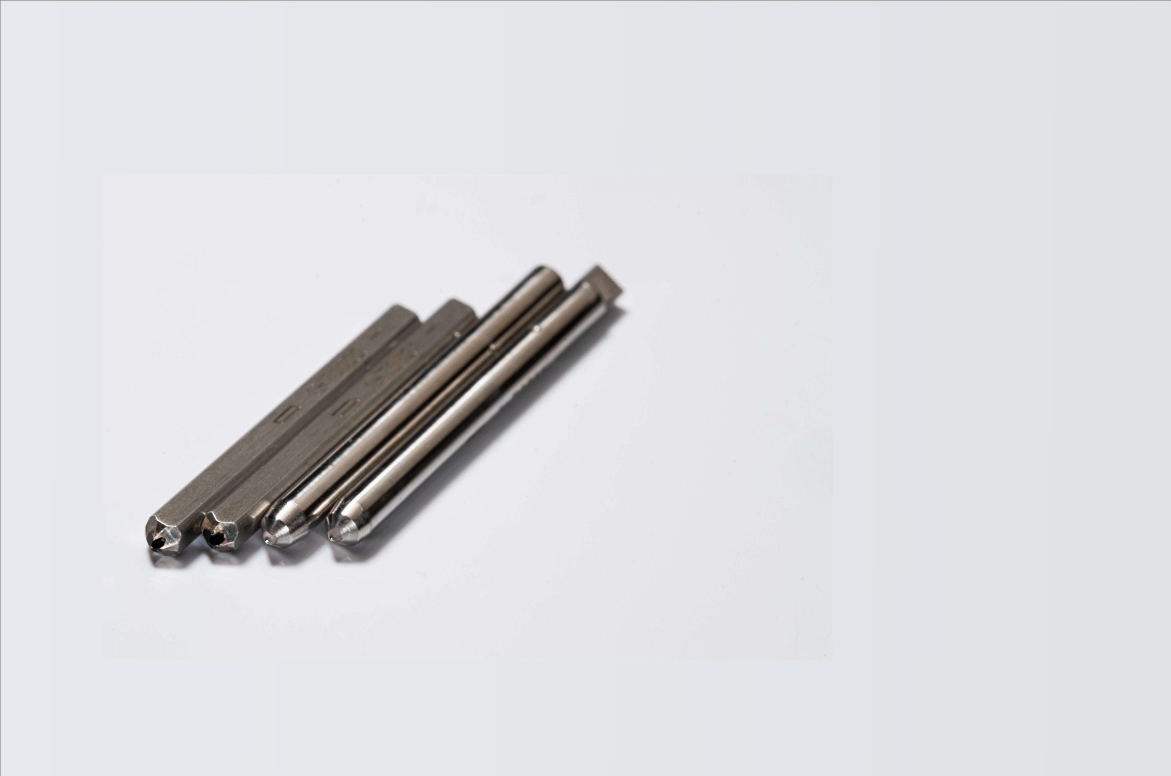
Laser die need to have both ends perpendicular to the direction of light and be smooth in order to increase luminous efficiency. Therefore, the scribe method that makes use of the cleave is standard for singulating InP wafers. Tecdia’s solution is a diamond scribe tool with a heel angle of 5 degrees, which is suitable for InP (Knoop hardness 460). The cutting edge of the high precision machined scribe tool does not touch any part of the electronic circuit and skillfully controls the propagating crack.
Tip shape stability is due to high diamond processing technology and stable mass production technology
Wafer chips are subject to more difficult processing conditions as the final product becomes smaller and has higher performance. Scribing technology and scribe equipment have not changed much over the years, with the quality of the diamond scribe tool itself greatly affecting the singulation precision. Since InP is a soft and delicate material, the effect is remarkable. For clients aiming for full automation, the mass production technology of Tecdia enables near-perfect diamond scriber production in large quantities with consistent quality.
Adopted for chipping process for 5G front hall
In addition to InP, Tecdia’s diamond scriber has a lineup of shapes that can be used to cut a wide range of materials such as GaAs, GaN, and SiC. We also can customize it to whatever you need. Please feel free to contact us if you are looking to use scribe tools for high precision singulation of wafer die.
Semiconductor electronic component manufacturer (semiconductor diode)
 +1-408-748-0100
Office Hours: 8:30am - 5:30pm PST