Silicon carbide wafers are difficult to cut because they are almost as hard as the diamond they are cut with. These wafers are also often brittle and easily chipped without the proper tools. Learn how Tecdia, your scribing specialist, came to the rescue of several semiconductor chip manufacturers.
Silicon carbide (SiC) is a material that has huge potentials to enrich our lives. Many types of devices are being developed using this material, and soon the world will start to produce SiC products on a large scale. However, there have been no mature singulation technologies that can handle this material for high-volume production. This tutorial presents a solution from our wafer scribing specialists.
The Problem
The prior issue/status
SiC wafers are very difficult to singulate using conventional methods.
The Solution
How the issue was solved
Improvement in scribing quality by changing the shapes of the cuts
Key Point
The reason for adoption
Not only do we singulate the sample wafer we receive from the client, we make it a point to discuss the specific results that are desired so that we can customize an existing product to your needs.
The Result
The effect of the solution
Manufacturers of SiC products have a new method of dicing wafers that produces high-yields at mass production rates.
The ProblemThe prior issue/status
SiC wafers are very difficult to singulate using conventional methods.

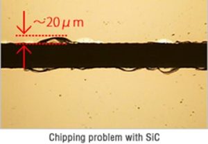
Silicon carbide (SiC) is the third hardest compound on the face of the earth, coming in at number 13 on the revised Mohs scale. Only diamonds and boron carbide (15 and 14 on the revised Mohs scale) are harder. Being so high on the Mohs scale makes dicing SiC wafers a difficult challenge. Cutting with a saw blade is slow, tedious, and can generate a lot of heat. Since the material is also brittle, chipping is also a common problem. Cutting with laser also has its own challenges such as debris and the fact that the machine is very expensive.

Because silicon carbide wafers are extremely hard and brittle, singulation is exceedingly slow and prone to excessive die edge chipping, which makes economical mass production difficult. The tools are also very expensive to replace. In order for semiconductor manufacturers to move from the SiC device development stage to profitable mass production, these singulation problems needed to be solved.

The SolutionHow the issue was solved
Improvement in scribing quality by changing the shapes of the cuts.
Since it’s impossible to change a diamond’s molecular hardness, we innovatively have changed the shape of the cutting edge of the diamond scribe tool tip.. We wanted to create an ideal scribing tool for SiC using our unique diamond polishing technology. At the same time, we started working on optimizing our wafer scribing equipment processes for use of the new scribing tool we were developing. It proved to be a winning combination. The improved scribing technique produced chip-free SiC die cuts with clean, straight lines. We not only solved the product quality and yield issues. We improved the process and achieved a higher production output.

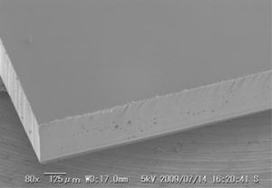
Diced Sic wafer die sample produced by improved scribing technique

Key PointThe reason for adoption

Not only do we singulate the sample wafer we receive from the client, we make it a point to discuss the specific results that are desired so that we can customize an existing product to your needs.

Tecdia’s new technology will enable a higher standard of quality and throughput than traditional saw dicing. Unsurprisingly, the equipment is also more economical than a laser scribe machine. There are several benefits to using our wafer scribing tools for SiC wafer singulation processing, and as scribing professionals it is our number one recommendation.

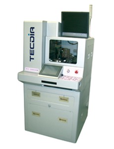
Wafer Scribing Machine


The ResultThe effect of the solution

Manufacturers of SiC products have a new method of dicing wafers that produces high-yields at mass production rates.

Client Information


【Client Industries】
Electrical, transportation, and power equipment manufacturing
【Business Description】
Manufacturing of semiconductor components


Related Sites


Contact

+1-408-748-0100
Office Hours: 8:30am - 5:30pm PST

Contact
...