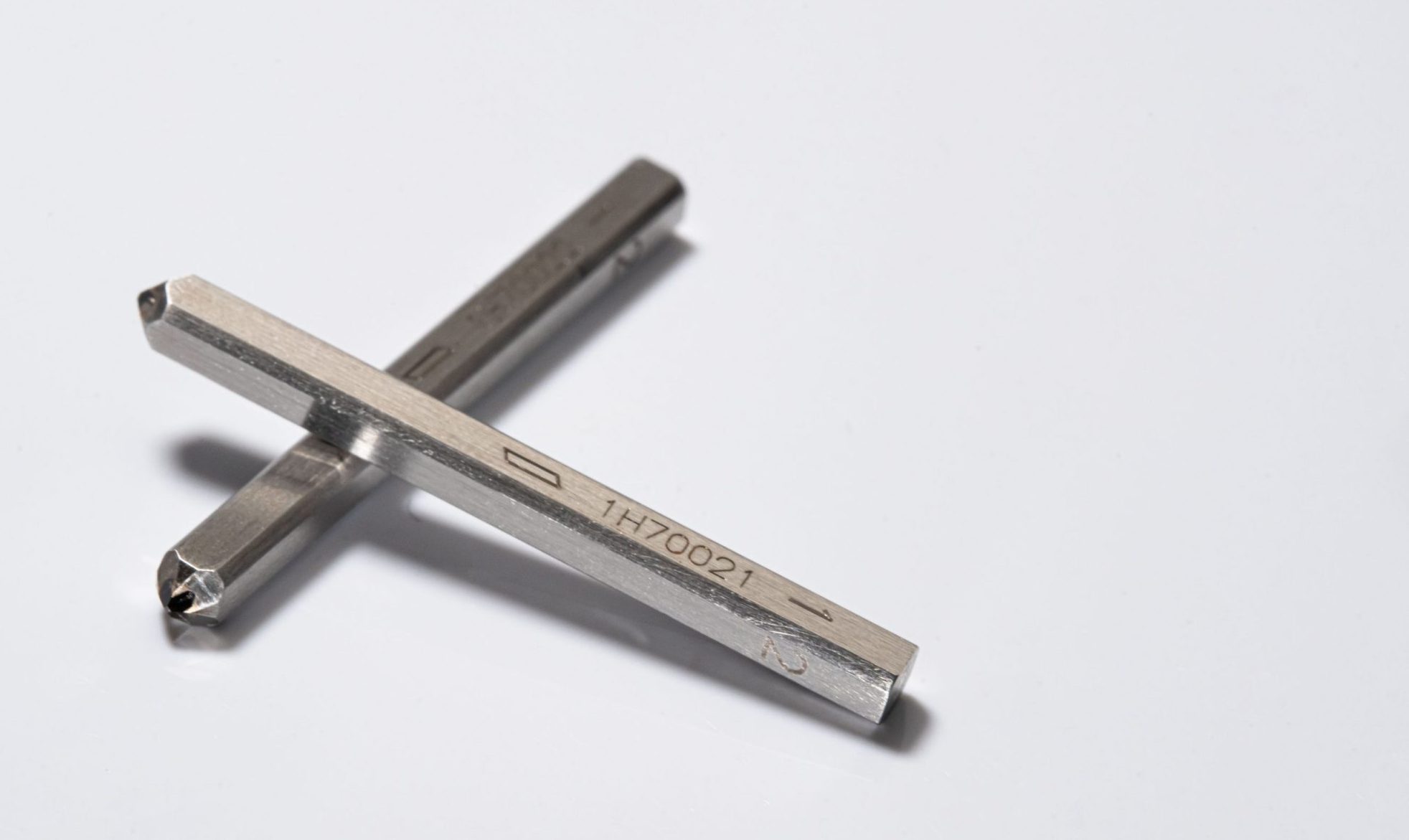


Singulating Grooved Wafers
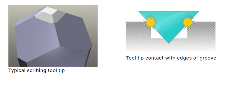
In today’s semiconductor market, there is continual demand for innovative product designs that extend beyond making chips from flat surface wafers. One example is a wafer fabrication process that results in each device chip built on the wafer being separated from the other chips by deep grooves, leaving the chips looking like “mesas” across the wafer landscape. Once fabricated, the wafer has to be diced in order to extract the semiconductor chips. But to scribe and break these wafers requires the cutting blade of the tool to scribe the bottom of the narrow and deep grooves (or wafer “streets”) with sufficient force to fracture the wafer without the tool contacting the edges of the chips.
If the ridgelines of the scribing tool hit the edge of the groove it can damage the chips or affect the tip’s penetration into the groove, fluctuating the required pressure for a fracture. It was clear that the semiconductor manufacturer needed a solution to overcome this challenge with the wafer singulation process.
Tecdia worked with a semiconductor manufacturer to investigate the unique characteristics of semiconductor wafers with grooves, i.e. “mesa chips.”
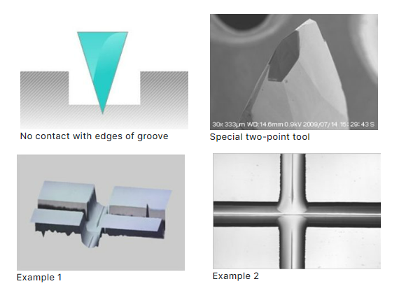
Based on what we learned, a special two-point diamond scribing tool would be narrow enough to avoid contact with the inside walls of the groove. Furthermore, this diamond scribing tool is strong enough to apply the necessary force and durable enough for mass production. After accepting our proposal, we built and tested the new tool design: a tool that provides ample clearance as it penetrates the base of the deep and narrow grooves. Samples of the tool were delivered to the semiconductor manufacturer for evaluation.
Tecdia’s scribing tool engineers and diamond-shaping technicians lived up to the high standards of our clientele.
It seems only natural that a world renowned manufacturer of diamond scribing tools and scribing equipment was able to provide an effective solution. In this case, the essential key to our success was partnering with someone who needed the solution.
Semiconductor manufacturers now have access to new scribing technology that will enable them to more efficiently mass produce products that require mesa wafer configurations.
 +1-408-748-0100
Office Hours: 8:30am - 5:30pm PST