

High Voltage Single Layer Capacitor
Creating a Single-layer ceramic capacitor that can withstand high voltage
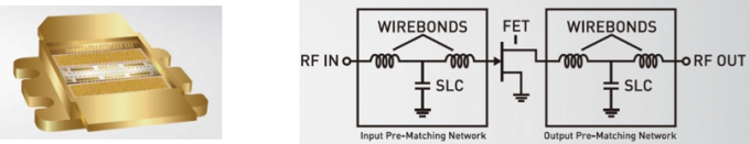
In GaN semiconductors, single-layer ceramic capacitors are also used for impedance matching and are used under high voltage on the drain side. Due to this, single-layer ceramic capacitors that can withstand high voltage are required. Since the amplified high-frequency voltage is superimposed in addition to the bias voltage, single-layer ceramic capacitors are required to withstand high voltage within the margin of the rated voltage.
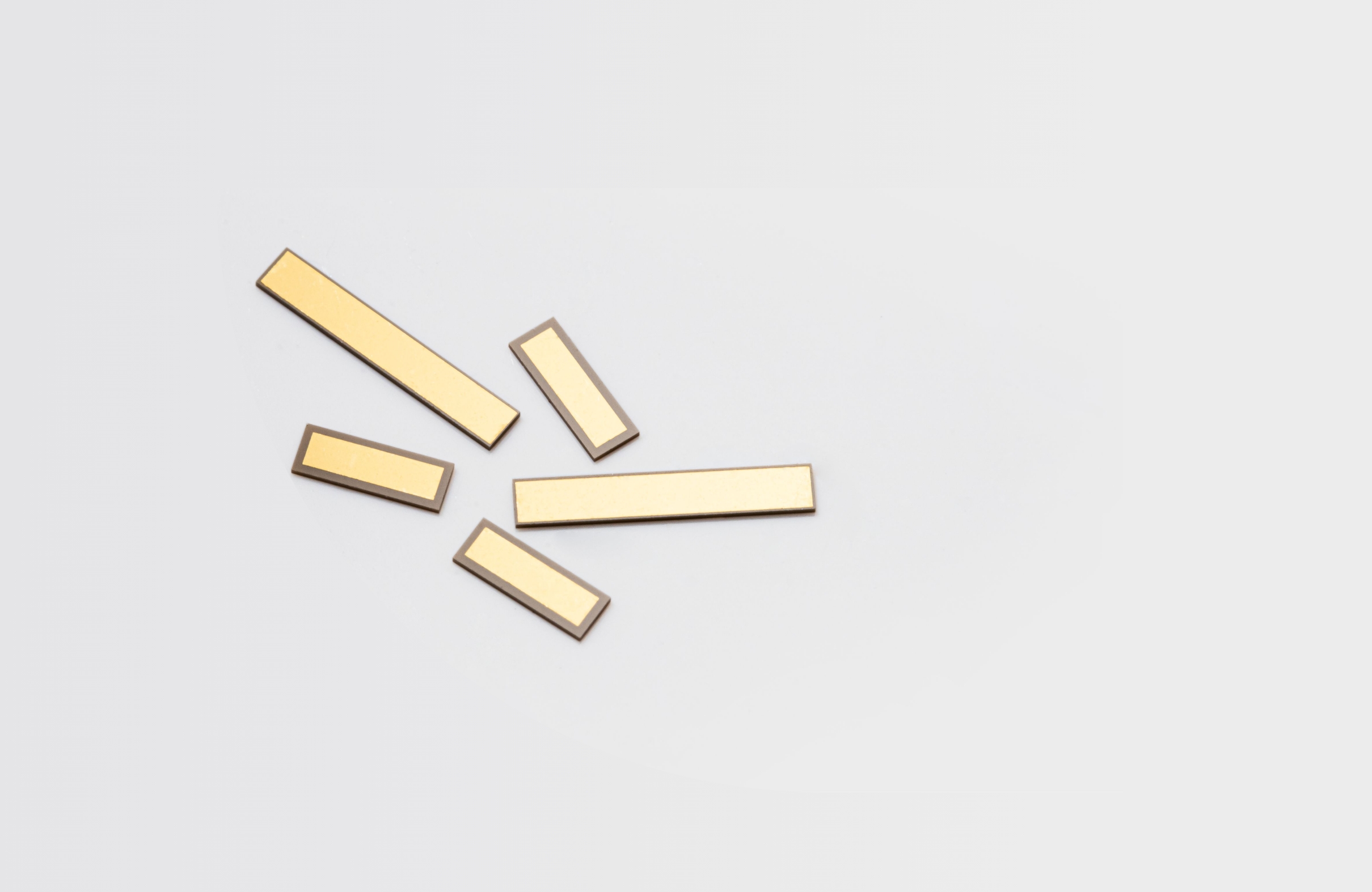
To manufacture single-layer ceramic capacitor with a rated voltage of 200V
In response to market needs, Tecdia has prototyped a high-voltage single-layer ceramic capacitor with the following specifications.
| Rated Voltage | 200V |
| Size | 3mmX1mm |
| Thickness | 0.15mm – 0.25mm |
| Capacitance | 5 pF- 50 pF |
Tecdia’s 200V capacitors have five features.
1. Achieves a breakdown voltage of 500V or higher, making it ideal for high-voltage applications
2. High reliability
3. By customizing to a rectangle, it is also possible to implement a horizontally long structure (L: W = maximum 8: 1)
4. Providing the optimum solution by customization of the size and capacity value
5. Conductive epoxy attachment protects heat-sensitive peripheral parts.
Consistent manufacturing from dielectric substrate manufacturing to mass production.
At Tecdia, we manufacture substrates with dielectric constants ranging from 40 to 50,000, which realize extremely high insulation properties suitable for withstanding high voltage, from kneading to firing in-house. Since we carry out everything from the manufacture of dielectric substrates to the mass production, we can customize the size and capacity value according to the customer needs.
Realization of High Efficiency Semiconductors
Tecdia has noticed the efficiency has been improved by optimizing the impedance using a high-voltage single-layer ceramic capacitor, as well as the power added efficiency (PAE) has improved compared to MOS capacitors.
Examples of applications for high-voltage single-layer ceramic capacitors are bias circuits and impedance matching for amplification semiconductors that go into defense radios. Currently, we do not have a lineup of high-voltage single-layer ceramic capacitors as regular products, but we can guide you through the full customization process. Please feel free to contact us.
–
 +1-408-748-0100
Office Hours: 8:30am - 5:30pm PST