Tecdia’s unique diamond processing and precision machining techniques produces best-in-class Berkovich Diamond Nanoindenters.
As thin-film technology becomes commonplace in the applied sciences of semiconductor, mass storage and microelectromechanical systems (MEMS) development, the precise characterization of these materials is a key element for R&D advancements. As designs become miniaturized from micro to nano and the demand for smaller and thinner products increases, the necessity for high quality precision tools becomes critical. Nanoindentation is a technique used to measure a material’s properties such as hardness or Young’s Modulus in an extremely small area or volume of material. Measurements are taken by pressing a small diamond-tipped shaft, called a Nanoindenter, directly into the sample where highly sophisticated lab equipment reads the pressure and analyzes the geometrical feedback. This technique can be used to measure properties in a wide variety of materials such as organic polymers, metals, ceramics, oxides, nitrides, and other carbon based elements. The performance and precision of the Nanoindenter is a critical factor for testing accuracy. Tecdia’s knowledge and experience in diamond processing and precision machining led to many improvements on existing designs.
The Problem
The prior issue/status
A superior product to meet the strict requirements of nanoindentation
The Solution
How the issue was solved
Combining diamond processing expertise and precision machining
Key Point
The reason for adoption
By combining our expertise in diamond processing and precision instrument production, Tecdia developed a need-based solution.
The Result
The effect of the solution
Supporting the advancement of innovation in the test and measurements industry
The ProblemThe prior issue/status
A superior product to meet the strict requirements of nanoindentation

Historically, improvement in tool precision and the production yield of nanoindentation tools has been a tremendous challenge.

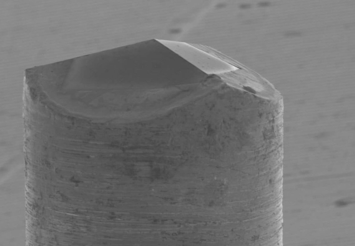
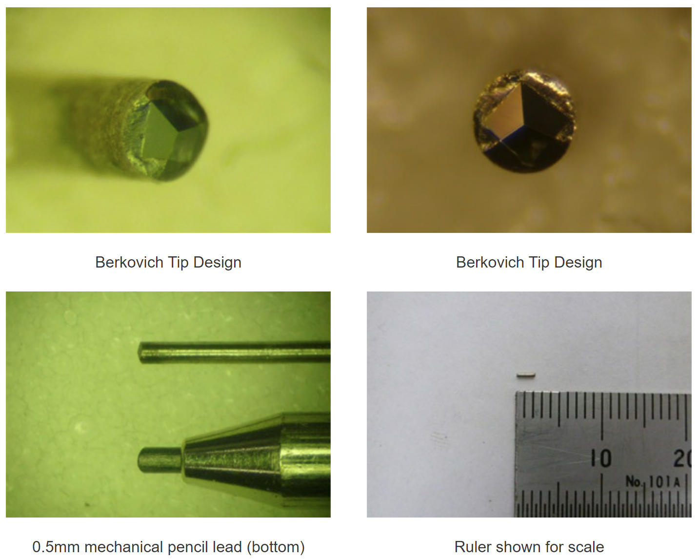
Nanoindenters consist of a diamond tip and Titanium or stainless steel shaft. The shaft diameter is typically less than 0.5mm and the total length is only 2 to 3mm long. The tip radius is less than 100 nanometers.

While diamond is the hardest material on Earth, they can be very brittle and difficult to work with at the microscopic level. Affixing the diamonds to the shaft with consistency and precision was also a challenge. Advancements in both shaping and mounting techniques were developed in order to attain consistent yields.

The SolutionHow the issue was solved
Combining diamond processing expertise and precision machining
Tecdia has successfully integrated diamond processing techniques along with our established history of precision machining.
Our expertise is backed with a proven 30 year track record for developing breakthrough diamond products such as phonograph needles, scalpels, and scribe tools for wafer singulation and also precision machining products like dispensing nozzles. These experiences have led us to develop high-quality, high-yield Nanoindenters for our customers.


Key PointThe reason for adoption

By combining our expertise in diamond processing and precision instrument production, Tecdia developed a need-based solution.

Not only were we able to exceed our customer’s expectations for precision, we were also able to increase the consistency of our product, in which high yields are crucial for continued satisfaction. Tecdia mobilized our expertise in mass production to provide a high-precision, best-in-class diamond Nanoindenter solution.

The ResultThe effect of the solution
Supporting the advancement of innovation in the test and measurements industry
Nanoindentation is increasingly used to understand and develop materials with improved methods of measuring ultra-low load friction coefficients and nanoscale adhesion. In achieving mass production of this solution, we increased our ability to support the increasing needs of our customers and therefore contribute to the advancement of the test and measurements industry.

Client Information

【Client Industries】
Electronics, Semiconductors, Biomedical, Material Sciences
【Business Description】
R&D, Test & Measurements


Related Sites

Contact

+1-408-748-0100
Office Hours: 8:30am - 5:30pm PST

Contact
...