

NASA Chooses Tecdia for Precision TaN Circuits
Patterning TaN with tight tolerances
In order for the sensor to operate within the earth’s atmosphere it must be under extreme vacuum and subjected to low temperatures approaching zero degrees Kelvin. Fine line patterning and tight tolerances were required for these accurate measurements. A line and space width of only 20 +/- 3 microns was essential.
All metals eventually become superconductive but at different temperatures. Instead of using Gold (Au) to make conductive traces, NASA engineers required Tantalum Nitride (TaN), a metal most commonly used for the manufacture of resistive circuits in optical and wireless transceivers. TaN becomes superconductive at a higher temperature making it far easier to maintain in a superconductive state.
When approaching zero degrees Kelvin, TaN has near zero resistance. This low level of resistance is ideal for circuits that need to detect extremely small environmental changes like the spin and magnetic fields of individual photons.
Tecdia’s TaN purity and adhesion exceeds expectations
Tecdia’s TaN material was chosen by NASA for its purity. They proved that it became superconducting around 1.2 Kelvin, a temperature that was within the cooling range of their 3 stage cooling chamber. Also in this extreme temperature environment the 20 micron traces and tolerances were stable due to our high metal adhesion and the use of low thermal expansion of 99.6% Alumina material. All of these benefits allowed NASA to develop this sensor to take sensitive measurements as required by the imaging system.
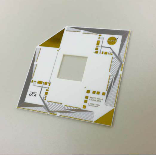
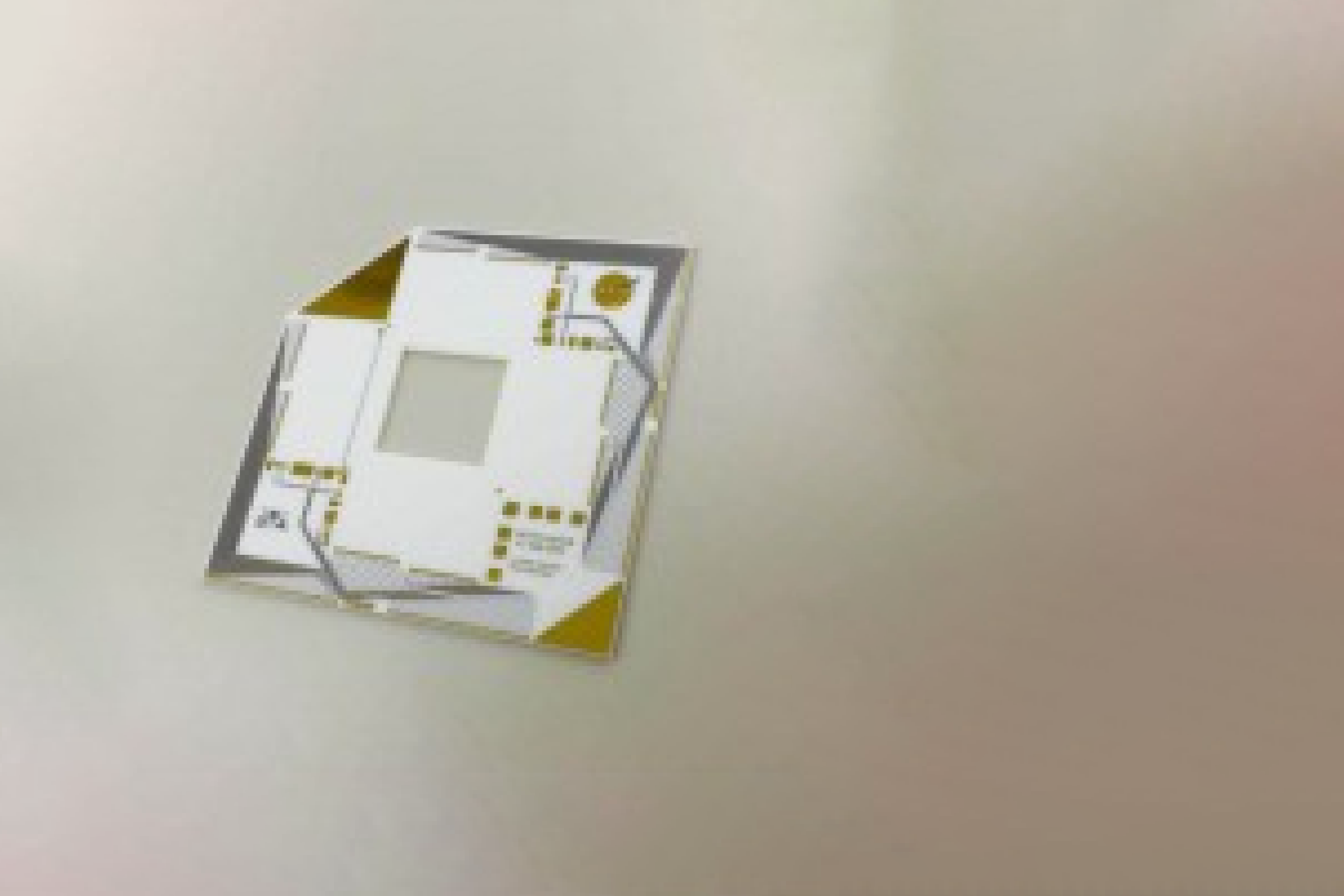
A 20 μm circuit board made of tantalum nitride.
NASA logo on the upper right and Tecdia logo on the lower left.
Etching and other processing technologies have made high-precision circuit boards possible.
Tecdia’s processing technology realized that 20μm thin and uniform tantalum nitride circuit was a great solution to utilize in this process.
In addition, Tecdia’s uncompromising stance of making samples in a short delivery time and going beyond the customer’s request was also a major reason for the decision to adopt this process.
The picture below shows the actual substrate with patterning in both TaN and Au.
The TaN traces (blue/grey color) can be seen surrounding the edges of the substrate which connect the gold wire bondable pads together. NASA is currently testing their image sensor which will be used for deep space exploration in the near future.
United States National Aeronautics and Space Administration (NASA)
 +1-408-748-0100
Office Hours: 8:30am - 5:30pm PST